Monday, December 16, 2013

Researchers split water into hydrogen, oxygen using light, nanoparticles

Researchers split water into hydrogen, oxygen using light, nanoparticles

Researchers from the University of Houston have found a catalyst that can quickly generate hydrogen from water using sunlight, potentially creating a clean and renewable source of energy.
Their research, published online Sunday in Nature Nanotechnology, involved the use of cobalt oxide nanoparticles to split water into hydrogen and oxygen.
Jiming Bao, lead author of the paper and an assistant professor in the Department of Electrical and Computer Engineering at UH, said the research discovered a new photocatalyst and demonstrated the potential of nanotechnology in engineering a material's property, although more work remains to be done.
Bao said photocatalytic water-splitting experiments have been tried since the 1970s, but this was the first to use cobalt oxide and the first to use neutral water under visible light at a high energy conversion efficiency without co-catalysts or sacrificial chemicals. The project involved researchers from UH, along with those from Sam Houston State University, the Chinese Academy of Sciences, Texas State University, Carl Zeiss Microscopy LLC, and Sichuan University.
Researchers prepared the nanoparticles in two ways, using femtosecond laser ablation and through mechanical ball milling. Despite some differences, Bao said both worked equally well.
Different sources of light were used, ranging from a laser to white light simulating the solar spectrum. He said he would expect the reaction to work equally well using natural sunlight.
Once the nanoparticles are added and light applied, the water separates into hydrogen and oxygen almost immediately, producing twice as much hydrogen as oxygen, as expected from the 2:1 hydrogen to oxygen ratio in H2O water molecules, Bao said.
The experiment has potential as a source of renewable fuel, but at a solar-to-hydrogen efficiency rate of around 5 percent, the conversion rate is still too low to be commercially viable. Bao suggested a more feasible efficiency rate would be about 10 percent, meaning that 10 percent of the incident solar energy will be converted to hydrogen chemical energy by the process.
Other issues remain to be resolved, as well, including reducing costs and extending the lifespan of cobalt oxide nanoparticles, which the researchers found became deactivated after about an hour of reaction.
"It degrades too quickly," said Bao, who also has appointments in materials engineering and the Department of Chemistry.
The work, supported by the Welch Foundation, will lead to future research, he said, including the question of why cobalt oxide nanoparticles have such a short lifespan, and questions involving chemical and electronic properties of the material.

University of Houston (2013, December 15). Researchers split water into hydrogen, oxygen using light, nanoparticlesScienceDaily. Retrieved December 16, 2013, from http://www.sciencedaily.com­/releases/2013/12/131215160904.htm?utm_source=feedburner&utm_medium=feed&utm_campaign=Feed%3A+sciencedaily%2Ftop_news%2Ftop_science+%28ScienceDaily%3A+Top+News+--+Top+Science%29

Thursday, November 21, 2013

Hydrogen cars could be headed to showroom near you

Cars that run on hydrogen and exhaust only water vapor are emerging to challenge electric vehicles as the world's transportation of the future.

At auto shows on two continents Wednesday, three automakers were unveiling hydrogen fuel cell vehicles to be delivered to the general public as early as spring of next year.
Korea's Hyundai Motor Co. will be the first to the mass market in the U.S. with a hydrogen-powered Tucson small SUV for lease next spring. Details were to come later Wednesday at the Los Angeles Auto Show. Honda also revealed plans in Los Angeles for a car due out in 2015. Earlier, at the Tokyo Motor Show, Toyota promised a mass-produced fuel cell car by 2015 in Japan and 2016 in the U.S.
Hydrogen cars are appealing because unlike electric vehicles, they have the range of a typical gasoline car and can be refueled quickly. Experts say the industry also has overcome safety and reliability concerns that have hindered distribution in the past.
But hydrogen cars still have a glaring downside—refueling stations are scarce, and costly to build. Critics say the cars are still a long way from mass production.
Consumers can expect costs in line with some luxury models. In Tokyo, Toyota promised a price of 5 million yen ($50,000) to 10 million yen ($100,000), and as close to the lower figure as possible. That's comparable to its Lexus sedans, but a range that makes the once space-age experiment with fuel cells more credible.
Even as battery-powered and hybrid-electric cars took on conventional gasoline models in the past decade, automakers continued research into hydrogen fuel cells, said Paul Mutolo, director of external partnerships for the Cornell University Energy Materials Center. Manufacturers now are limited only by costs and the lack of filling stations, he said.
Hydrogen cars, Mutolo said, have an advantage over battery-powered electric cars because drivers don't have to worry about running out of electricity and having to wait hours for recharging. "It's very similar to the kind of behavior that drivers have come to expect from their gasoline cars," he said.
Hydrogen fuel cells use a complex chemical process to separate electrons and protons in hydrogen gas molecules. The electrons move toward a positive pole, and the movement creates electricity. That powers a car's electric motor, which turns the wheels. "You're literally ripping the electrons from inside the molecule, generating electricity," Mutolo said.
Since the hydrogen isn't burned, there's no pollution. Instead, oxygen also is pumped into the system, and when it meets the hydrogen ions and electrons, that creates water and heat. The only byproduct is water. A fuel cell produces only about one volt of electricity, so many are stacked to create enough juice.
Hydrogen costs as little as $3 for an amount needed to power a car the same distance as a gallon of gasoline, Mutolo said.
Hyundai's plan includes leasing the hydrogen SUVs starting in the Los Angeles area, where most of the state's nine refueling stations are located. California lawmakers have allocated $100 million to build 100 more.
Mutolo estimates it will take at least 10 years for stations to spread nationwide.
Manufacturers likely will lose money on hydrogen cars at first, but costs will decrease as precious metals are reduced in the fuel cells, he said.
Toyota said its new fuel cell vehicle will be for ordinary customers, not just officials and celebrities. The car will go on sale in Japan in 2015 and within a year later in Europe and U.S.
Toyota's fuel cell car is on display as a "concept" model called FCV at the Tokyo show, where alternative fuel is grabbing the spotlight. The FCV looks ready to hit the streets, similar to the Prius gas-electric hybrid.
Honda, which has leased about two-dozen fuel cell cars since 2005, took the wraps off a futuristic-looking FCEV concept vehicle in Los Angeles. The concept vehicle shows the style of a 300-mile range fuel cell car that will be marketed in the U.S. and Japan in 2015 and in Europe after that. Honda wouldn't say if it will be offered for lease or purchase.
All major automakers, including General Motors Co. and Daimler, have been working on fuel cells for decades. But the prospect of reaching showrooms was not very real until recently.
Skeptics say hydrogen-fueling stations are more expensive than electric car charging stations, partly because electricity is almost everywhere and new and safe ways for producing, storing and transferring hydrogen will be needed.
Carlos Ghosn, chief executive of Nissan Motor Co., which has bet heavily on electric vehicles for its future, is one vocal skeptic.
"Having a prototype is easy. The challenge is mass-marketing," he told reporters. He said he did not see a mass-market fuel cell as viable before 2020.


Read more at: http://phys.org/news/2013-11-hydrogen-cars-showroom.html#jCp

Tuesday, September 24, 2013

Lowering the power consumption of CNT-based CMOS devices to subnanowatt

Researchers have demonstrated a new carbon nanotube (CNT)-based logic device that consumes just 0.1 nanowatts (nW) in its static ON and OFF states, representing the lowest reported value by 3 orders of magnitude for CNT-based CMOS logic devices. The device could serve as a building block for large-area, ultralow-power CNT logic circuits that can be used to realize a variety of nanoelectronics applications.

The researchers, Michael L. Geier, et al., at Northwestern University in Evanston, Illinois, and the University of Minnesota in Minneapolis, have published their paper on the subnanowatt CNT logic in a recent issue of Nano Letters.

'As the researchers explain, one of the biggest advantages of CMOS architecture is that it has intrinsically low power consumption. This benefit arises from the fact that, unlike other logic architectures, one of the two types of transistors (p-type or n-type) is turned off under steady state conditions in each logic gate in CMOS devices.
In order to fully take advantage of this potential for extremely low power consumption, the p-type and n-type transistors need to have precisely tuned and well-separated threshold voltages, which are the voltage levels that determine whether the device is ON or OFF. So far, this issue of the threshold voltages has not been addressed, and the researchers here identified it as the key challenge limiting the realization of highly integrated CNT-based CMOS electronics.

In their study, the researchers used a metal gate structure to achieve symmetric and clearly separated threshold voltages for p-type and n-type CNT transistors, resulting in the ultralow power consumption. In the static states, in which the device is either ON or OFF, power consumption is less than 0.1 nW. At the midpoint of the transfer state, when both p-type and n-type transistors are simultaneously in the ON state, the voltage reaches its peak at 10 nW.'
By connecting multiple CNT transistors in various configurations, the researchers demonstrated inverter, NAND and NOR logic gates. In the future, these gates can be integrated into complex circuits, where they can provide subnanowatt static power consumption along with the other advantages of CNTs, such as solution processability and flexibility.


More information: Michael L. Geier, et al. "Subnanowatt Carbon Nanotube Complementary Logic Enabled by Threshold Voltage Control." Nano LettersDOI: 10.1021/nl402478p


Monday, September 23, 2013

Creating electricity with caged atoms

Clathrates are crystals consisting of tiny cages in which single atoms can be enclosed. These atoms significantly alter the material properties of the crystal. By trapping cerium atoms in a clathrate, scientists at the Vienna University of Technology have created a material which has extremely strong thermoelectric properties. It can be used to turn waste heat into electricity.

A lot of energy is wasted when machines turn hot, unnecessarily heating up their environment. Some of this  could be harvested using ; they create electric current when they are used to bridge hot and cold objects. At the Vienna University of Technology (TU Vienna), a new and considerably more efficient class of thermoelectric materials can now be produced. It is the material's very special  that does the trick, in connection with an astonishing new physical effect; in countless tiny cages within the crystal, cerium atoms are enclosed. These trapped magnetic atoms are constantly rattling the bars of their cage, and this rattling seems to be responsible for the material's exceptionally favourable properties.
Cerium Cages from the Mirror Oven
"Clathrates" is the technical term for , in which host atoms are enclosed in cage-like spaces. "These clathrates show remarkable thermal properties", says Professor Silke BĂĽhler-Paschen (TU Vienna). The exact behaviour of the material depends on the interaction between the trapped atoms and the cage surrounding them. "We came up with the idea to trap cerium atoms, because their  promised particularly interesting kinds of interaction", explains BĂĽhler-Paschen.
For a long time, this task seemed impossible. All earlier attempts to incorporate magnetic atoms such as the  cerium into the clathrate structures failed. With the help of a sophisticated crystal growth technique in a mirror oven, Professor Andrey Prokofiev (TU Vienna) has now succeeded in creating clathrates made of barium, silicon and gold, encapsulating single cerium atoms.

Electricity from Temperature Differences
The  of the novel material have been tested. Thermoelectrics work when they connect something hot with something cold: "The thermal motion of the electrons in the material depends on the temperature", explains BĂĽhler-Paschen. "On the hot side, there is more thermal motion than on the cold side, so the electrons diffuse towards the colder region. Therefore, a voltage is created between the two sides of the thermoelectric material."
Experiments show that the cerium atoms increase the material's thermopower by 50%, so a much higher voltage can be obtained. Furthermore, the thermal conductivity of clathrates is very low. This is also important, because otherwise the temperatures on either side would equilibrate, and no voltage would remain.
The World's Hottest Kondo Effect

"The reason for these remarkably good  seem to lie in a special kind of electron-electron correlation – the so-called Kondo effect", Silke BĂĽhler-Paschen believes. The electrons of the cerium atom are quantum mechanically linked to the atoms of the crystal. Actually, the Kondo effect is known from low temperature physics, close to absolute zero temperature. But surprisingly, these quantum mechanical correlations also play an important role in the novel clathrate materials, even at a temperature of hundreds of degrees Celcius.
"The rattling of the trapped cerium  becomes stronger as the temperature increases", says BĂĽhler-Paschen. "This rattling stabilizes the Kondo effect at high temperatures. We are observing the world's hottest Kondo effect."
More Research for Better and Cheaper Clathrates
The research team at TU Vienna will now try to achieve this effect also with different kinds of clathrates. In order to make the material commercially more attractive, the expensive gold could possibly be substituted by other metals, such as copper. Instead of cerium, a cheaper mixture of several rare-earth elements could be used. There are high hopes that such designer clathrates can be technologically applied in the future, to turn industrial  into valuable electrical energy.


Read more at: http://phys.org/news/2013-09-electricity-caged-atoms.html#jCp

More information: Thermopower enhancement by encapsulating cerium in clathrate cages, DOI: 10.1038/nmat3756

Friday, September 20, 2013

Graphene could yield cheaper optical chips

Optoelectronic devices built from graphene could be much simpler in design than those made from other materials. If a method for efficiently depositing layers of graphene—a major area of research in materials science—can be found, it could ultimately lead to optoelectronic chips that are simpler and cheaper to manufacture.

"Another advantage, besides the possibility of making  simpler, is that the high mobility and ultrahigh carrier-saturation velocity of electrons in graphene makes for very fast detectors and modulators," says Dirk Englund, the Jamieson Career Development Assistant Professor of Electrical Engineering and Computer Science at MIT, who led the new research.
Graphene is also responsive to a wider range of light frequencies than the materials typically used in photodetectors, so graphene-based optoelectronic chips could conceivably use a broader-band optical signal, enabling them to move data more efficiently. "A two-micron photon just flies straight through a germanium photodetector," Englund says, "but it is absorbed and leads to measurable current—as we actually show in the paper—in graphene."


Read more at: http://phys.org/news/2013-09-graphene-yield-cheaper-optical-chips.html

More information: http://www.nature.com/nphoton/journal/vaop/ncurrent/full/nphoton.2013.253.html

Thursday, September 19, 2013

Smartphone as a 'Microscope' to detect a single virus and nanoparticles

With the emerging of cutting edge technology of smartphone as Samsung Galaxy, Iphone etc, your smartphone now can see what the naked eye cannot: A single virus and bits of material less than one-thousandth of the width of a human hair.
Aydogan Ozcan, a professor of electrical engineering and bioengineering at the UCLA Henry Samueli School of Engineering and Applied Science, and his team have created a portable smartphone attachment that can be used to perform sophisticated field testing to detect viruses and bacteria without the need for bulky and expensive microscopes and lab equipment. The device weighs less than half a pound.
"This cellphone-based imaging platform could be used for specific and sensitive detection of sub-wavelength objects, including bacteria and viruses and therefore could enable the practice of nanotechnology and biomedical testing in field settings and even in remote and resource-limited environments," Ozcan said. "These results also constitute the first time that single nanoparticles and viruses have been detected using a cellphone-based, field-portable imaging system."
The new research, published on Sept. 9 in the American Chemical Society's journal ACS Nano, comes on the heels of Ozcan's other recent inventions, including a cellphone camera-enabled sensor for allergens in food products and a smart phone attachment that can conduct common kidney tests.
Capturing clear images of objects as tiny as a single virus or a nanoparticle is difficult because the optical signal strength and contrast are very low for objects that are smaller than the wavelength of light.
In the ACS Nano paper, Ozcan details a fluorescent microscope device fabricated by a 3-D printer that contains a color filter, an external lens and a laser diode. The diode illuminates fluid or solid samples at a steep angle of roughly 75 degrees. This oblique illumination avoids detection of scattered light that would otherwise interfere with the intended fluorescent image.
Using this device, which attaches directly to the camera module on a smartphone, Ozcan's team was able to detect single human cytomegalovirus (HCMV) particles. HCMV is a common virus that can cause birth defects such as deafness and brain damage and can hasten the death of adults who have received organ implants, who are infected with the HIV virus or whose immune systems otherwise have been weakened. A single HCMV particle measures about 150-300 nanometers; a human hair is roughly 100,000 nanometers thick.
In a separate experiment, Ozcan's team also detected nanoparticles -- specially marked fluorescent beads made of polystyrene -- as small as 90-100 nanometers.
To verify these results, researchers in Ozcan's lab used other imaging devices, including a scanning electron microscope and a photon-counting confocal microscope. These experiments confirmed the findings made using the new cellphone-based imaging device.
Ozcan is the principal investigator on the research. The first author of ACS Nano the paper is Qingshan Wei, a postdoctoral researcher in Ozcan's lab and at UCLA's California NanoSystems Institute (CNSI), where Ozcan is associate director. Other co-authors include Hangfei Qi and Ting-Ting Wu of the UCLA Department of Molecular and Medical Pharmacology; Wei Luo, Derek Tseng, Zhe Wan and Zoltan Gorocs of the UCLA Electrical Engineering Department; So Jung Ki of the UCLA Department of Chemistry and Biochemistry; Laurent Bentolila of CNSI and the UCLA Department of Chemistry and Biochemistry; and Ren Sun of the UCLA Department of Molecular and Medical Pharmacology and CNSI.


Unbreakable and flexible phone is on the edge...

Breakthrough research at RMIT University is advancing transparent bendable electronics, bringing science fiction gadgets – such as unbreakable rubber-like phones, rollable tablets and even functional clothing – closer to real life.
Researchers from RMIT’s Functional Materials and Microsystems research group have developed a new method to transfer electronics with versatile functionality, which are usually made on rigid silicon, onto a flexible surface.

The result of their work is published today (13 September) in Nature Publishing Group’s Asia Materials, the leading materials science journal for the Asia-Pacific.
The ability of micro and nano-electronic devices to sense, insulate or generate energy is controlled by thin, transparent nanolayers of oxide materials, often much thinner than 1/100th of a human hair.
These oxide materials are brittle and their high processing temperatures – often in excess of 300 °C – have until now prevented their incorporation in flexible electronic devices.
Lead author, PhD researcher Philipp Gutruf, said the new process developed at RMIT could unleash the potential of fully functional flexible electronics, while providing a new way for the materials to mesh together.
"We have discovered a micro-tectonic effect, where microscale plates of oxide materials slide over each other, like geological plates, to relieve stress and retain electrical conductivity," he said.
"The novel method we have developed overcomes the challenges of incorporating oxide materials in bendable electronic devices, paving the way for bendable consumer electronics and other exciting applications."
Supervisor and co-leader of the research group, Dr Madhu Bhaskaran, said the new approach used two popular materials – transparent conductive indium tin oxide and rubber-like silicone which is also biocompatible.
“The ability to combine any functional oxide with this biocompatible material creates the potential for biomedical devices to monitor or stimulate nerve cells and organs. This is in addition to the immediate potential for consumer electronics applications in flexible displays, solar cells, and energy harvesters.”
Mr Gutruf is supported by an Australian Government Endeavour International Postgraduate Research Scholarship and the research was supported by Australian Post-Doctoral Fellowships from the Australian Research Council to Dr Bhaskaran and Dr Sharath Sriram, co-leader of the research group.


Wednesday, September 18, 2013

Autonomic Restoration of Electrical Conductivity

Self-healing of an electrical circuit is demonstrated with nearly full recovery of conductance less than one millisecond after damage. Crack damage breaks a conductive pathway in a multilayer device, interrupting electron transport and simultaneously rupturing adjacent microcapsules containing gallium–indium liquid metal (top). The released liquid metal flows to the area of damage, restoring the conductive pathway (bottom).

Autonomic Restoration of Electrical Conductivity Blaiszik 2011 Advanced Materials Wiley Online Library

Tuesday, September 17, 2013

Self-Healing Polymer 'Terminator Polymer'

This is a neat trick. After slicing a tube of gelatinous material in half with a razor, researchers stick the two pieces back together again. After they've sat together for two hours at room temperature, the pieces are impossible to pull apart. The material, a new invention, has healed itself:


Self-healing materials like this would be useful in so many places. They could keep tablets, phones and other everyday objects from sustaining nicks and scratches. Even NASA studies self-healing materials because they could reduce the need for costly and dangerous repairs in tough environments, i.e., space. Many labs around the world are working on different versions of this.
The material shown above, invented by a team of materials scientists from the IK4-CIDETEC Research Center in Spain, is one of the first that is able to heal itself without the help of heat, light, added chemicals or other interventions, according to Chemistry World. (Self-healing materials often need some kind of catalyst to trigger the changes in chemistry required to bond broken pieces back together again.)

Sunday, September 15, 2013

Wednesday, September 11, 2013

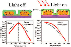
Shining a little light changes metal into semiconductor

          
By blending their expertise, two materials science engineers at Washington University in St. Louis changed the electronic properties of a new class of materials — just by exposing it to light.
With funding from the Washington University International Center for Advanced Renewable Energy and Sustainability (I-CARES), Parag Banerjee, PhD, and Srikanth Singamaneni, PhD, both assistant professors of materials science, brought together their respective areas of research.

Singamaneni’s area of expertise is in making tiny, pebble-like nanoparticles, particularly gold nanorods. Banerjee’s area of expertise is making thin films. They wanted to see how the properties of both materials would change when combined.

The research was published online in August in ACS Applied Materials & Interfaces.
The research team took the gold nanorods and put a very thin blanket of zinc oxide, a common ingredient in sunscreen, on top to create a composite. When they turned on light, they noticed that the composite had changed from one with metallic properties into a semiconductor, a material that partly conducts current. Semiconductors are commonly made of silicon and are used in computers and nearly all electronic devices.
“We call it metal-to-semiconductor switching,” Banerjee said. “This is a very exciting result because it can lead to opportunities in different kinds of sensors and devices.”
Banjeree said when the metallic gold nanorods are exposed to light, the electrons inside the gold get excited and enter the zinc oxide film, which is a semiconductor. When the zinc oxide gets these new electrons, it starts to conduct electricity.
“We found out that the thinner the film, the better the response,” he said. “The thicker the film, the response goes away. How thin? About 10 nanometers, or a 10 billionth of a meter.”
Other researchers working with solar cells or photovoltaic devices have noticed an improvement in performance when these two materials are combined; however, until now, none have broken it down to discover how it happens, Banerjee said.
“If we start understanding the mechanism for charge conduction, we can start thinking about applications,” he said. “We think there are opportunities to make very sensitive sensors, such as an electronic eye. We are now looking to see if there is a different response when we shine a red, blue or green light on this material.”
Banerjee also said this same technology can be used in solar cells.

Source:  Wu F, Tian L, Kanjolia R, Singamaneni S, Banerjee P. Plasmonic Metal-to-Semiconductor Switching in Au Nanorod-ZnO nanocomposite films. ACS Applied Materials & Interfaces. Dx.doi.org/10.1021/am402309x.


Monday, September 9, 2013

Stanford scientists use DNA to assemble a transistor from graphene

Stanford scientists use DNA to assemble a transistor from graphene

DNA meets electronics

DNA is the blueprint for life. Could it also become the template for making a new generation of computer chips based not on silicon, but on an experimental material known as graphene?
That's the theory behind a process that Stanford chemical engineering professor Zhenan Bao reveals in Nature Communications.

Bao and her co-authors, former post-doctoral fellows Anatoliy Sokolov and Fung Ling Yap, hope to solve a problem clouding the future of electronics: consumers expect silicon chips to continue getting smaller, faster and cheaper, but engineers fear that this virtuous cycle could grind to a halt.
Why has to do with how silicon chips work.
Everything starts with the notion of the semiconductor, a type of material that can be induced to either conduct or stop the flow of electricity. Silicon has long been the most popular semiconductor material used to make chips.
The basic working unit on a chip is the transistor. Transistors are tiny gates that switch electricity on or off, creating the zeroes and ones that run software.
To build more powerful chips, designers have done two things at the same time: they've shrunk transistors in size and also swung those gates open and shut faster and faster.
The net result of these actions has been to concentrate more electricity in a diminishing space. So far that has produced small, faster, cheaper chips. But at a certain point, heat and other forms of interference could disrupt the inner workings of silicon chips.
"We need a material that will let us build smaller transistors that operate faster using less power," Bao said.
Graphene has the physical and electrical properties to become a next-generation semiconductor material – if researchers can figure out how to mass-produce it.
Graphene is a single layer of carbon atoms arranged in a honeycomb pattern. Visually it resembles chicken wire. Electrically this lattice of carbon atoms is an extremely efficient conductor.
Bao and other researchers believe that ribbons of graphene, laid side-by-side, could create semiconductor circuits. Given the material's tiny dimensions and favorable electrical properties, graphene nano ribbons could create very fast chips that run on very low power, she said.
"However, as one might imagine, making something that is only one atom thick and 20 to 50 atoms wide is a significant challenge," said co-author Sokolov.
To handle this challenge, the Stanford team came up with the idea of using DNA as an assembly mechanism.
Physically, DNA strands are long and thin, and exist in roughly the same dimensions as the graphene ribbons that researchers wanted to assemble.
Chemically, DNA molecules contain carbon atoms, the material that forms graphene.
The real trick is how Bao and her team put DNA's physical and chemical properties to work.
The researchers started with a tiny platter of silicon to provide a support (substrate) for their experimental transistor. They dipped the silicon platter into a solution of DNA derived from bacteria and used a known technique to comb the DNA strands into relatively straight lines.
Next, the DNA on the platter was exposed to a copper salt solution. The chemical properties of the solution allowed the copper ions to be absorbed into the DNA.
Next the platter was heated and bathed in methane gas, which contains carbon atoms. Once again chemical forces came into play to aid in the assembly process. The heat sparked a chemical reaction that freed some of the carbon atoms in the DNA and methane. These free carbon atoms quickly joined together to form stable honeycombs of graphene.
"The loose carbon atoms stayed close to where they broke free from the DNA strands, and so they formed ribbons that followed the structure of the DNA," Yap said.
So part one of the invention involved using DNA to assemble ribbons of carbon. But the researchers also wanted to show that these carbon ribbons could perform electronic tasks. So they made transistors on the ribbons.
"We demonstrated for the first time that you can use DNA to grow narrow ribbons and then make working transistors," Sokolov said.
The paper drew praise from UC Berkeley associate professor Ali Javey, an expert in the use of advanced materials and next-generation electronics.
"This technique is very unique and takes advantage of the use of DNA as an effective template for controlled growth of electronic materials," Javey said. "In this regard the project addresses an important research need for the field."
Bao said the assembly process needs a lot of refinement. For instance, not all of the carbon atoms formed honeycombed ribbons a single atom thick. In some places they bunched up in irregular patterns, leading the researchers to label the material graphitic instead of graphene.
Even so, the process, about two years in the making, points toward a strategy for turning this carbon-based material from a curiosity into a serious contender to succeed silicon.
"Our DNA-based fabrication method is highly scalable, offers high resolution and low manufacturing cost," said co-author Yap. "All these advantages make the method very attractive for industrial adoption."

Wednesday, July 24, 2013

Two-in-one solution for low cost polymer LEDs and solar cells

Two-in-one solution for low cost polymer LEDs and solar cells

July 22, 2013 — Considerable improvement in device performance of polymer-based optoelectronic devices is reported today by researchers from Ulsan National Institute of Science and Technology (UNIST), South Korea. The new plasmonic material, can be applied to both polymer light-emitting diodes (PLEDs) and polymer solar cells (PSCs), with world-record high performance, through a simple and cheap process.

The contrary demands of these devices mean that there are few metal nanoparticles that can enhance performance in PLEDs and PSCs at the same time.
Most semiconducting optoelectronic devices (OEDs), including photodiodes, solar cells, light emitting diodes (LEDs), and semiconductor lasers, are based on inorganic materials. Examples include gallium nitride for light-emitting diodes and silicon for solar cells.
Due to the limited availability of raw materials and the complex processing required to manufacture OEDs based on inorganic materials, the cost of device fabrication is increasing. There is great interest in thin-film OEDs that are made from alternative semiconductors.
Among these materials, organic semiconductors have received much attention for use in next-generation OEDs because of the potential for low-cost and large-area fabrication using solution processing.
Despite extensive efforts to develop new materials and device architectures enhancing the performance of these devices, further improvements in efficiency are needed, before there can be widespread use and commercialization of these technologies.
The material prepared by the UNIST research team is easy to synthesize with basic equipment and has low-temperature solution processability. This low-temperature solution processability enables roll-to-roll mass production techniques and is suitable for printed electronic devices.

Journal Reference:
  1. Hyosung Choi, Seo-Jin Ko, Yuri Choi, Piljae Joo, Taehyo Kim, Bo Ram Lee, Jae-Woo Jung, Hee Joo Choi, Myoungsik Cha, Jong-Ryul Jeong, In-Wook Hwang, Myoung Hoon Song, Byeong-Su Kim, Jin Young Kim. Versatile surface plasmon resonance of carbon-dot-supported silver nanoparticles in polymer optoelectronic devicesNature Photonics, 2013; DOI: 10.1038/nphoton.2013.181

Scientists break record for thinnest light-absorber: May lead to more efficient, cheaper solar cells

Scientists break record for thinnest light-absorber: May lead to more efficient, cheaper solar cells

July 18, 2013 — Stanford University scientists have created the thinnest, most efficient absorber of visible light on record. The nanosize structure, thousands of times thinner than an ordinary sheet of paper, could lower the cost and improve the efficiency of solar cells, according to the scientists.

Their results are published in the current online edition of the journal Nano Letters.
"Achieving complete absorption of visible light with a minimal amount of material is highly desirable for many applications, including solar energy conversion to fuel and electricity," said Stacey Bent, a professor of chemical engineering at Stanford and a member of the research team. "Our results show that it is possible for an extremely thin layer of material to absorb almost 100 percent of incident light of a specific wavelength."
Thinner solar cells require less material and therefore cost less. The challenge for researchers is to reduce the thickness of the cell without compromising its ability to absorb and convert sunlight into clean energy.
For the study, the Stanford team created thin wafers dotted with trillions of round particles of gold. Each gold nanodot was about 14 nanometers tall and 17 nanometers wide.

Journal Reference:
  1. Carl Hägglund, Gabriel Zeltzer, Ricardo Ruiz, Isabell Thomann, Han-Bo-Ram Lee, Mark L. Brongersma, Stacey F. Bent. Self-Assembly Based Plasmonic Arrays Tuned by Atomic Layer Deposition for Extreme Visible Light AbsorptionNano Letters, 2013; 13 (7): 3352 DOI:10.1021/nl401641v